This is an old revision of the document!
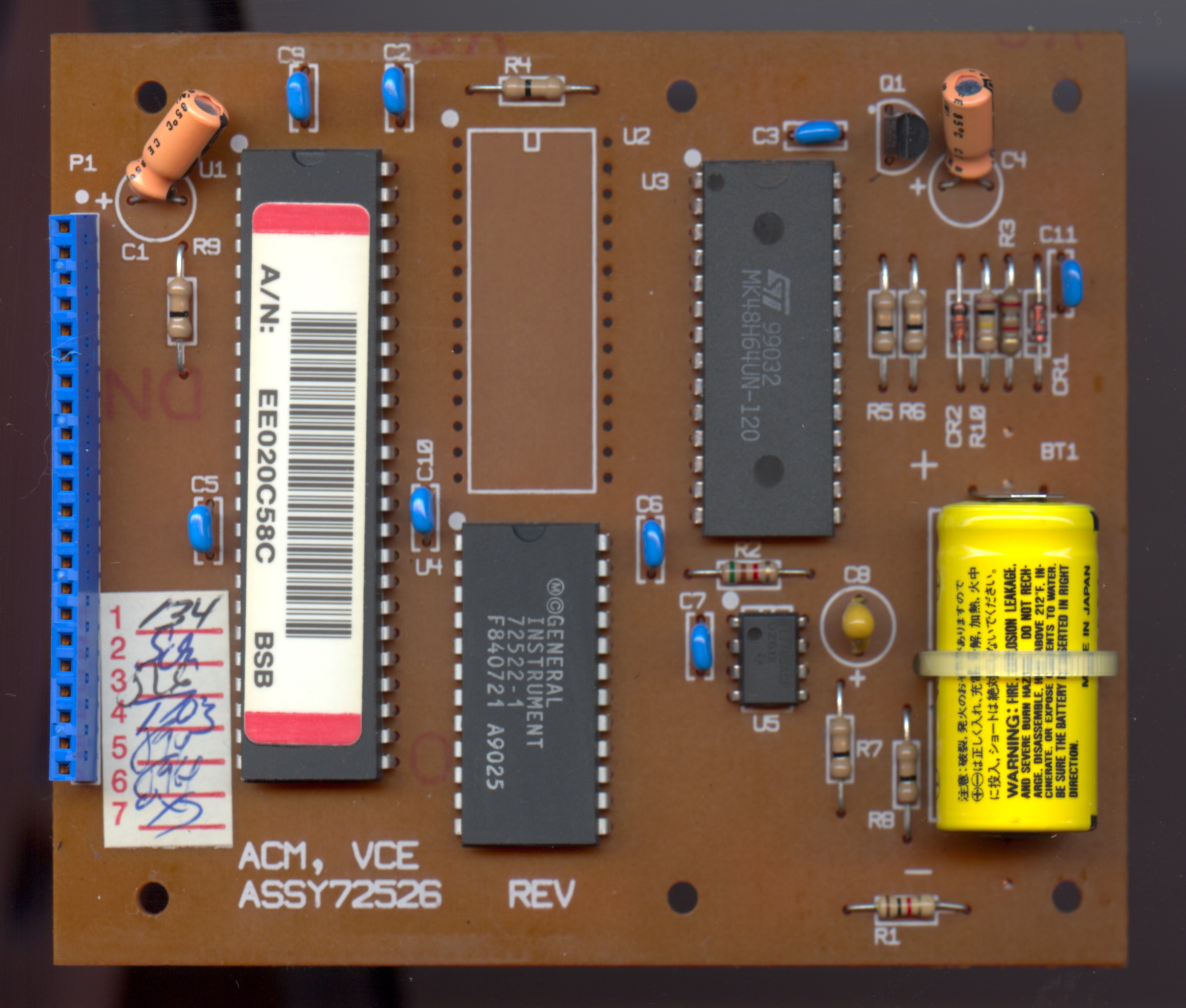
ACM hardware
Photos

Hardware description
The ACM is a relatively simple board with only four major components:
- NCR-manufactured custom ASIC
- General Instrument part number
72523-2F840590 A9023 - Western Design Centre embedded CMOS 6502 CPU core with extended instructions
- 8-bit parallel (6502-style) interface to communicate with the set-top box
- Serial ACM-bus interface to communicate with e.g. an external modem for impulse pay-per-view features
 Possibly some kind of encryption processor
- The key only changes every 256 frames (~10 seconds), so this doesn't have to be particularly fast.
- According to (ref: Bennett, Moroney and Cutts, “The Architecture and Security Design Goals of the Eurocypher system”), the algorithm used is proprietary to Eurocypher. This is unlike VideoCipher II, which uses DES.
- (ref: Chippindale and Franks, “Dished!”) suggests that the algorithm change may have been done at the behest of the NSA and GCHQ.
- Signetics 27C256 OTP EPROM (main program code)
- General Instrument part number
72524-2(V1.20 V1.50firmware) or72524-5(V1.50firmware)
- 8-kbyte low-power RAM, with battery back-up
- Either a Mostek/ST MK48H64LN-120 or MK48H64UN-120 (most common) or Fujitsu 8464A-20L.
- General Instrument
72522-1OSD controller- 16 lines of 31 characters
- Display attributes seem to be per-line. According to (ref: Bennett, Moroney and Cutts, “The Architecture and Security Design Goals of the Eurocypher system”):
- Text is always white; font supports upper and lower case characters.
- Double height, underline and blinking.
- Background transparent (TV picture show-thru), blue or black, with shadowing or blocking of characters.
- The RGB output and OSD Enable (fast blanking) is fed to the VCU2133 video processor in the receiver.
Memory map
| Start address | End address | Assigned to |
|---|---|---|
0x0000 | 0x1FFF | 8Kbytes battery-backed RAM (U3) |
0x2000 | 0x3FFF | The reset routine accesses addresses 0x2100-0x2102 and 0x2401. |
0x4000 | 0x7FFF | OSD chip (U4) note only A0 and A1 are connected to U4 |
0x8000 | 0xFFFF | 32Kbytes EPROM (U2) |
ACM board pinout
| Pin | Function | Pin name (Ferguson) | Notes |
|---|---|---|---|
| 1 | GND | ||
| 2 | Ext ACM Data | PPV | Connects to external ACM peripherals, e.g. Videocipher VideoPAL |
| 3 | +5V | +5VA | |
| 4 | Interrupt | SIRQ | “Interrupt generated by the ACM” Philips: 8051 P3.3 (INT1) Tatung: 80C562 pin 26 (INT0) Ferguson: CCU3000 pin 60 |
| 5 | Register select | SIRS | “Used to switch between Control or Data for the ACM” Philips: A11 Tatung: 80C562 pin 28 (P3.4/T0) Ferguson: CCU3000 pin 46 |
| 6 | ACM select | SIACMSEL | “Select/strobe line used to select the ACM, which is used as if it were memory” Philips: 74F139 pin 9 (3b) Tatung: 80C562 pin 30 and 31 (/WR and /RD) Ferguson: CCU3000 pin 45 |
| 7 | Read/write | SIR/W | “Read/Write control for the ACM” Philips: A12 Tatung: 80C562 pin 29 (P3.5/T1) Ferguson: CCU3000 pin 47 |
| 8 | AD0 | DB0 | Data bus Philips: CPU data bus Tatung: 80C562 pin 50-57 (P0.7-P0.0) Ferguson: CCU3000 pin 48 to 55 (Port 7) |
| 9 | AD1 | DB1 | |
| 10 | AD2 | DB2 | |
| 11 | AD3 | DB3 | |
| 12 | AD4 | DB4 | |
| 13 | AD5 | DB5 | |
| 14 | AD6 | DB6 | |
| 15 | AD7 | DB7 | |
| 16 | CLK | CLK (SHAPED) | ACM clock, 20.25MHz Philips: Burst Clock Output from DMA2280 pin 60. =MCLK or MCLK/2 Tatung: clock buffer output; 4 x colourburst freq = 20.25MHz Ferguson: 20.25MHz clock, shaped with TTL gates |
| 17 | CSYNC IN | SYNC | Philips: from net “C9” (CSYNC) – which doesn't seem to go anywhere Tatung: “A” – DMA2280 pin 53 (CSYNC OUT) Ferguson: SYNC |
| 18 | Philips: 10nF to GND Tatung: R580 (1k) to “B” (PL702/PL752 pin 6 - Composite Sync out to MC1377) Ferguson: open |
||
| 19 | OSD Enable | OSDEN | To VCU2133 FB/R/G/B In pins |
| 20 | OSD Red | ROSD | |
| 21 | OSD Green | GOSD | |
| 22 | OSD Blue | BOSD |
Dumping the ROM
The ROM may be dumped by desoldering the chip and placing it into an EPROM eraser. Be careful not to short any of the pins or solder joints, as this may clear or corrupt the RAM contents.
Dumping the RAM
I'm investigating ways to dump the RAM. There are several options.
Piggy-back board
This option involves a piggy-back board which plugs into the EPROM socket. This would carry the EPROM, a Dallas DS1225 battery-backed RAM chip, and some logic ICs.
- The DS1225 is preprogrammed to known values, then fitted to the socket. The EPROM is installed, and the piggy-back board is fitted into the ACM.
- A wire would be soldered to RAM pin 27 to pick up the RAM write signal (
/RAMWR). - Logic would:
- Convert
/CS1andCS2(from the MK48H64 RAM) into a single/CSchip select signal for the DS1225. - Merge
/OEand/WRinto a single/WEwrite signal for the DS1225.
- This would mean any access to the RAM would result in a copy to the DS1225.
The disadvantage with this option is that only accessed RAM locations would be backed up. Essentially, this assumes that the ACM firmware does some kind of checksum or access of the RAM data when it boots.
Modified firmware and piggy-back board
This method involves building a piggy-back board with an FTDI FT245 USB-FIFO chip, an EPROM, and some glue logic.
- Accesses to the lower part of the EPROM cause a byte to be latched into the FT245.
- The EPROM code sends a short sync message, then reads the contents of RAM and sends it to the host via the FT245.
- Optional: add a means of reading from the FT245, allowing the RAM to be cloned.
This is a more involved option, but would allow the entire RAM to be dumped and restored as needed.
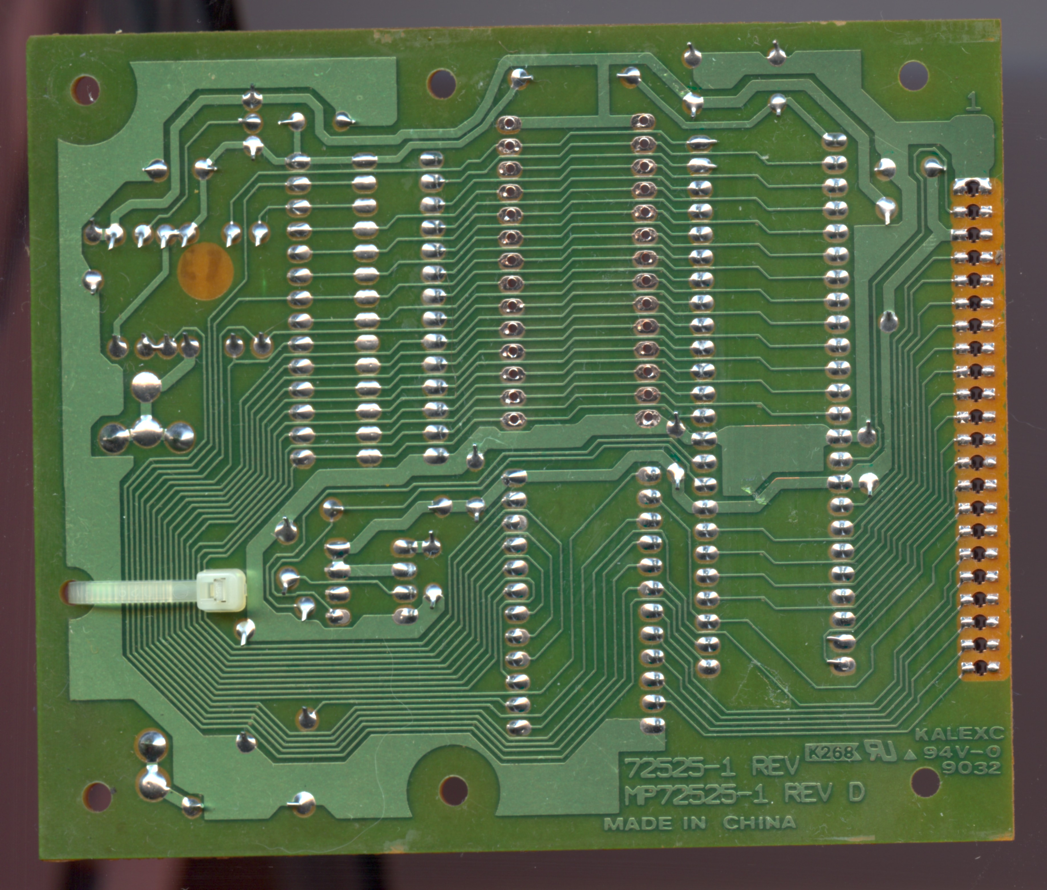
PCB layout
These two scans show the PCB in more detail. The PCB is single-sided, and these can be used to derive a schematic diagram.